Home / Applications / Materials Science Applications / Examination of semiconductor wafers | Configured Microscopes
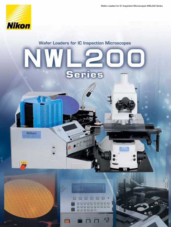
Nikon | IC Wafer Loader NWL200 – Advanced Wafer Loader for Inspection Microscopes
Nikon's latest innovation, the NWL200, sets new standards in inspection technology, designed specifically for use with inspection microscopes. The NWL200 series is the first to safely handle ultra-thin wafers with a thickness of just 100 micrometers.
Nikon Corporation
Nikon | IC Wafer Loader NWL200 – Advanced Wafer Loader for Inspection Microscopes
Nikon Corporation1-5-20 Nishioi, Shinagawa-ku
Tokyo 140-8601
Japan
Phone: +81 3 3773 1111
Phone Sales: +49 211 9414 888
Email Sales:
Email Service:
Web: https://www.microscope.healthcare.nikon.com/
Quote request
ManufacturerNikon Corporation
The request is sent to the manufacturer. The request is sent directly.
Description
With its advanced clamping system, these devices ensure reliable loading processes, making them ideal for next-generation semiconductor inspections. Enhanced features, such as automatic wafer detection, reduce the risk of damage to semiconductor disks. Additionally, the integrated edge crack detection system automatically identifies defects caused by edge damage.
The NWL200 series by Nikon represents precision, safety, and innovation, offering an essential solution for modern semiconductor inspections.
Technical Data:
| Category | Description |
|---|---|
| Model | NWL200 |
| Wafer Thickness | Up to 100 micrometers |
| Key Features | Advanced clamping system, automatic wafer detection, edge crack detection |
| Application Area | Semiconductor inspection, inspection microscopes |